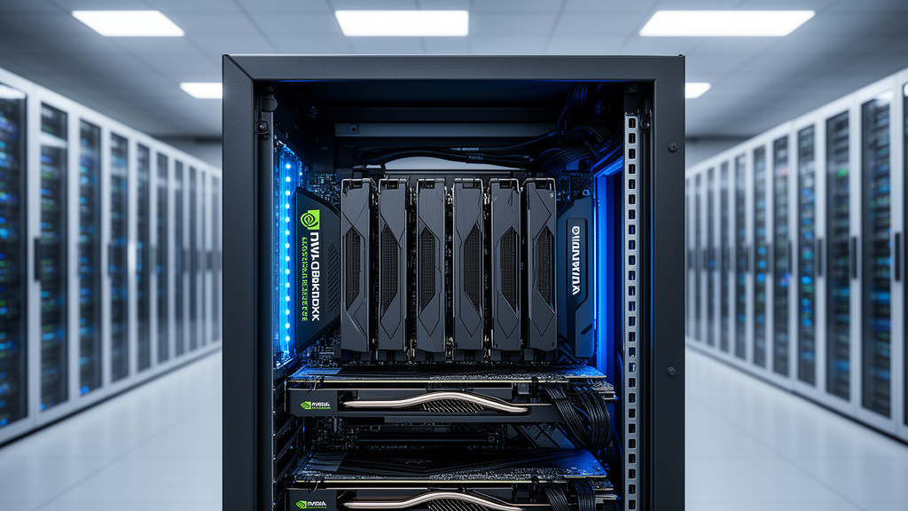
NVIDIA’s introduction of the Blackwell Ultra architecture marks a decisive evolution in the race to scale artificial intelligence infrastructure. By focusing heavily on computational efficiency and memory bandwidth, NVIDIA is directly tackling the primary bottleneck currently hindering hyper-scale data center operators: the ‘power wall.’ With a headline claim of 3x efficiency over the previous Hopper generation, the Blackwell Ultra is not merely a speed update; it is a fundamental shift in how massive AI models will be trained and deployed through 2025 and beyond.
Key Highlights
- Hyper-Scale Optimization: Engineered specifically for the next wave of trillion-parameter AI models requiring massive parallel processing power.
- 3x Efficiency Milestone: Significant architectural improvements allow for triple the energy efficiency compared to the Hopper-based H100/H200 deployments.
- HBM3e Integration: Leverages advanced High Bandwidth Memory to solve the critical memory-compute bottleneck in large-scale inference tasks.
- Accelerated Roadmap: The announcement underscores NVIDIA’s aggressive move to refresh its architecture annually, maintaining a dominant lead over emerging custom-silicon competitors.
The Architecture of Acceleration: Beyond Raw Compute
The AI sector has moved past the phase where raw FLOPS (Floating Point Operations Per Second) were the only metric that mattered. As models like GPT-4, Claude 3.5, and Llama 3 continue to balloon in size, the constraints on data centers have shifted toward energy consumption, cooling infrastructure, and memory latency. The Blackwell Ultra architecture responds directly to these constraints by reimagining the memory-compute interface.
The Memory Bottleneck and HBM3e
One of the most profound challenges in modern AI is feeding data to the GPU fast enough. If a processor can compute faster than it can receive data, it sits idle—a waste of electricity and infrastructure costs. The Blackwell Ultra utilizes enhanced HBM3e (High Bandwidth Memory) to dramatically increase the ‘pipe’ through which data flows. This ensures that the massive logic cores at the heart of the Blackwell GPU remain fully utilized. By reducing latency, NVIDIA allows operators to squeeze significantly more inference cycles out of the same power footprint compared to the previous H100 generation.
Efficiency as an Economic Imperative
In the era of hyper-scale computing, electricity is the largest operating expense. A 3x increase in efficiency is not just an environmental win; it is a massive economic lever for data center operators like Microsoft Azure, AWS, and Google Cloud. By lowering the power-per-inference metric, NVIDIA effectively lowers the barrier to entry for deploying agents and complex AI applications. This efficiency gain is achieved through a combination of smaller process node advancements and optimized interconnects between the Blackwell chips, reducing the ‘chatter’ that typically consumes energy in massive GPU clusters.
The Competitive Landscape: NVIDIA vs. Custom Silicon
This announcement also serves as a strategic defensive move against the rise of custom AI silicon. Giants like Google (with their TPUs) and Amazon (with Trainium) have been aggressively developing in-house chips to mitigate their reliance on NVIDIA’s hardware. The Blackwell Ultra’s aggressive performance-per-watt profile is designed to maintain NVIDIA’s ‘TCO’ (Total Cost of Ownership) advantage. Even with the costs associated with NVIDIA hardware, the sheer efficiency gains of the Blackwell Ultra suggest that it will remain the most cost-effective path for the world’s most demanding AI workloads.
The Future of AI Infrastructure
As we look toward 2025, the Blackwell Ultra acts as a bridge. It acknowledges that the era of ‘growth at all costs’ is ending, replaced by an era of ‘sustainable scaling.’ The industry can no longer just add more GPUs to a rack; they must ensure that every watt of electricity is converted into useful intelligence. NVIDIA’s move signals that they understand the infrastructure bottleneck is now a physical and economic one, and they are pivoting their engineering resources to address the real-world constraints of the modern data center.
FAQ: People Also Ask
Q: When will Blackwell Ultra chips be available for data centers?
A: NVIDIA has signaled that the Blackwell Ultra roadmap aligns with 2025 deployment schedules, keeping pace with the rapid cycle of AI infrastructure refresh rates currently seen across major cloud providers.
Q: How does the 3x efficiency claim compare to the H100?
A: The 3x efficiency improvement is calculated based on specific inference workloads. By optimizing the memory architecture (HBM3e) and interconnect bandwidth, the system completes more tasks per unit of power consumed compared to the Hopper architecture.
Q: Is Blackwell Ultra a completely new chip or a refresh of Blackwell?
A: Blackwell Ultra represents a high-performance enhancement of the core Blackwell architecture. It focuses on pushing the limits of the existing platform’s memory capacity and power efficiency rather than an entirely new, ground-up design.
Q: Will this impact the cost of running AI models?
A: Yes, theoretically. By increasing efficiency, data center operators can perform more inference cycles with the same power budget, which should lower the unit cost of training and deploying high-parameter models over time.